- التسوق ، اصبح سهلا.
- /
- احصل على التطبيق!
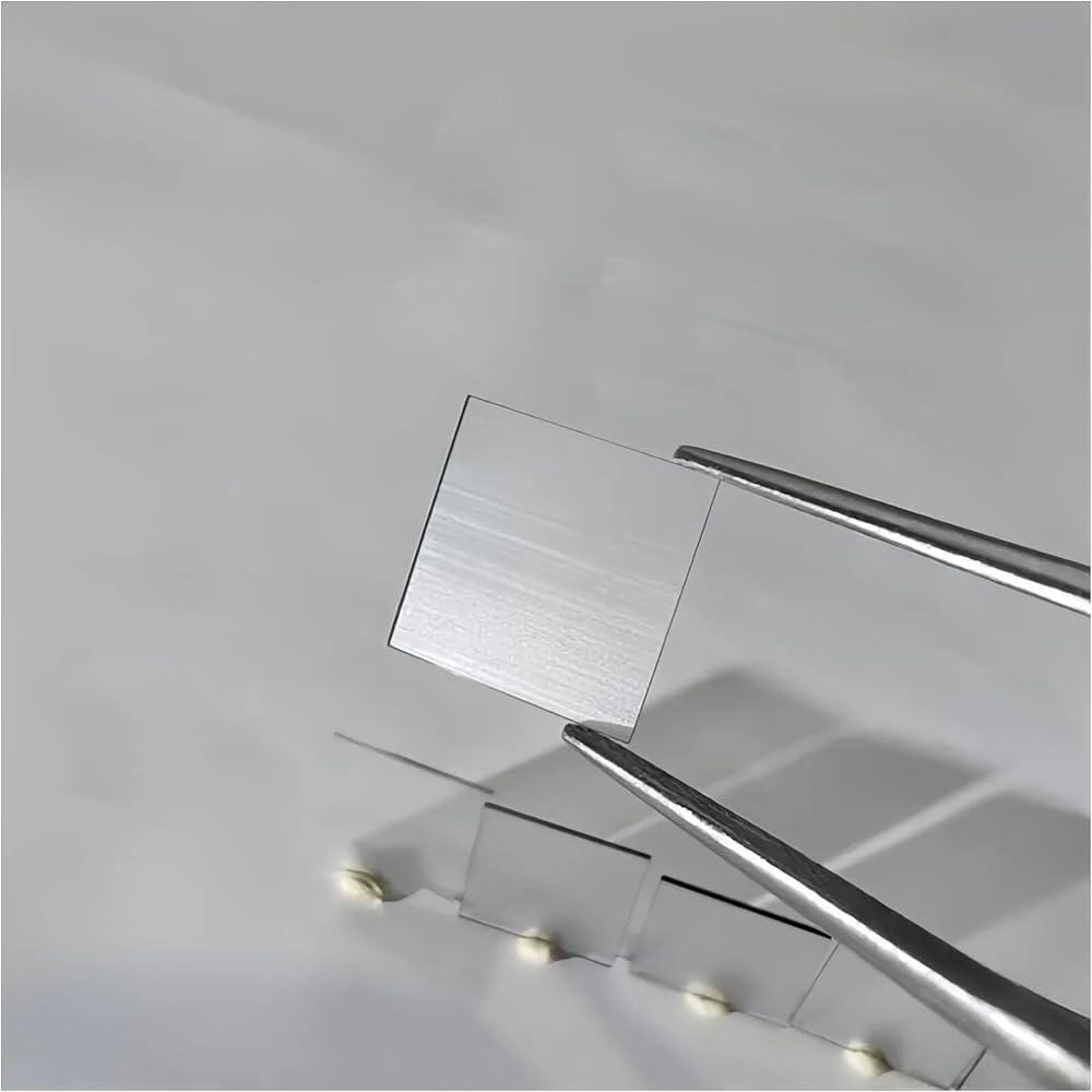
CVD Single-Crystal Diamond Seed Wafer (MP Substrate) is fabricated via chemical vapor deposition process. This double-side polished square diamond plate serves as homoepitaxial growth seed, semiconductor thermal substrate, high-power laser heat sink and laboratory research specimen.
The single-crystal lattice structure delivers low impurity content and stable batch consistency. Each wafer is precision cut with flat surface and tight dimensional tolerance. Double-sided mirror polishing effectively reduces defects during diamond epitaxial growth. Featuring high thermal conductivity, excellent electrical insulation and stable physical and chemical properties, these wafers support long-term operation under high-load working conditions.
Available standard sizes:
3×3mm (1/8"×1/8"),
4×4mm (5/32"×5/32"),
5×5mm (3/16"×3/16"),
6×6mm (1/4"×1/4"),
7×7mm (9/32"×9/32"),
8×8mm (5/16"×5/16"),
9×9mm (11/32"×11/32"),
10×10mm (3/8"×3/8"),
11×11mm (7/16"×7/16").
Each wafer is individually packaged with foam cushion in transparent case to prevent chipping and scratching. Widely used for MPCVD diamond growth, semiconductor chip thermal management, laser device heat dissipation and material science laboratory tests.
 طقم بيجامة نسائي من MOYEE قميص وسروال قصير الأكمام ناعم مكون من قطعتين طقم ملابس صالة مع جيوب
KWD 6
 طقم بيجامة حريمي من MOYEE من الساتان الناعم برقبة على شكل حرف V وسروال قصير مكون من قطعتين مع جيوب
KWD 8.500
 طقم بيجامة حريرية للسيدات من MOYEE مصنوع من الساتان مكون من قطعتين، قميص وسروال حريري مع جيوب
KWD 8.500
 قميص قصير من الحرير من MOYEE بدون أكمام كاجوال من الساتان بلوزة كاميس صيفية للنساء 2024
KWD 5.500

 الكويت
