- Shopping, made easy.
- /
- Get the app!
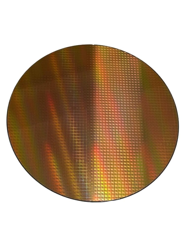
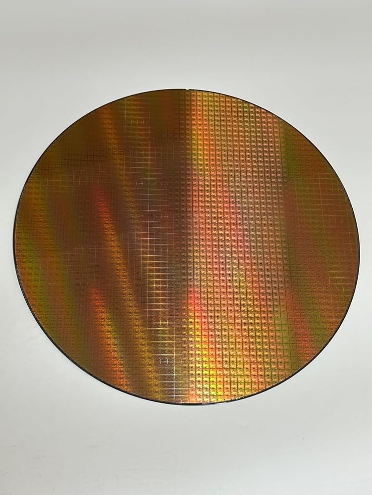
Product DescriptionThis integrated circuit wafer sample features visible semiconductor circuit patterns designed for display, demonstration and educational applications. The patterned surface provides a visual representation of wafer-level circuit layouts used in microelectronics manufacturing.
Suitable for equipment demonstrations, semiconductor training, engineering education and technology exhibitions, the wafer serves as a reference sample for illustrating integrated circuit fabrication concepts and semiconductor processing workflows.
The wafer can be incorporated into laboratory presentations, training programs, exhibition displays and technical showcases where a representative semiconductor circuit sample is needed.
Type: Integrated Circuit Pattern Wafer
Size Options: 8 Inch / 12 Inch
Application: Equipment Demonstration, Semiconductor Training, Technology Exhibition and Educational Display
 1-100mm Round Quartz Glass Disc 0.5mm Thin UV Optical Fused Silica (Φ15mm* 0.5mm *5pcs) | Round quartz glass discs with 1-100mm diameter and 0.5mm thickness, UV transparent, heat resistant optical substrates.
KWD 7.500
1-100mm Round Quartz Glass Disc 0.5mm Thin UV Optical Fused Silica (Φ15mm* 0.5mm *5pcs) | Round quartz glass discs with 1-100mm diameter and 0.5mm thickness, UV transparent, heat resistant optical substrates.
KWD 7.500
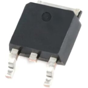 NCE0224K NCE2030K NCE3020K NCE3065K NCE60P12K NCE0224 NCE2030 NCE3020 NCE3065 NCE60P12 TO-252 IC 10Pcs(NCE3065K)
KWD 12
NCE0224K NCE2030K NCE3020K NCE3065K NCE60P12K NCE0224 NCE2030 NCE3020 NCE3065 NCE60P12 TO-252 IC 10Pcs(NCE3065K)
KWD 12
 1PCS SW16PCR055 Stud diode
KWD 16
1PCS SW16PCR055 Stud diode
KWD 16
 C5750X7R2A475M - Fixed 2 SMD 5750X7R2A475 (10 Piece Lot)
KWD 7
C5750X7R2A475M - Fixed 2 SMD 5750X7R2A475 (10 Piece Lot)
KWD 7