- التسوق ، اصبح سهلا.
- /
- احصل على التطبيق!
Description:
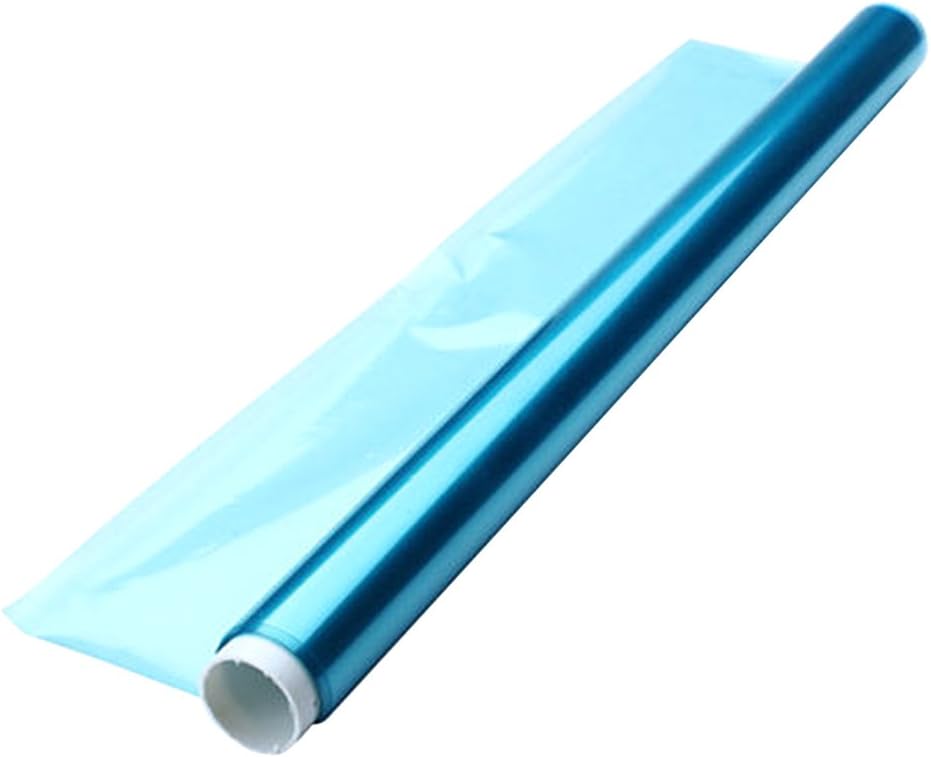
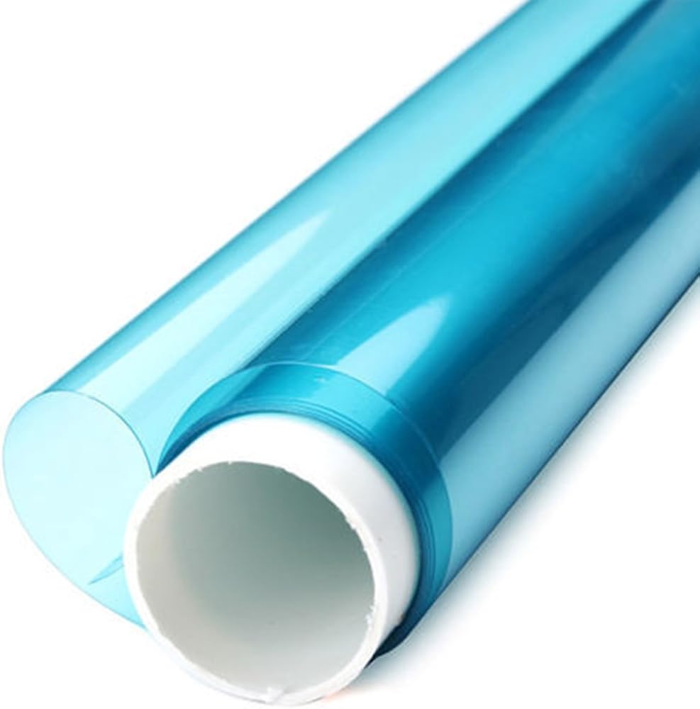
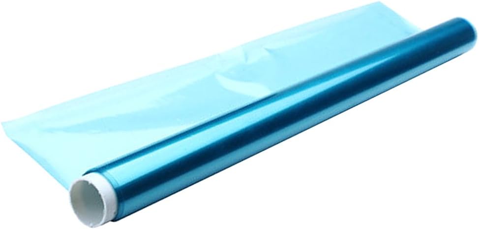
- Photographic film, also known as dry film, is used to make PCB board,stick it on top of the PCB, it will become a sensitive circuit board.
- Suitable for plating, hole covering??and the etching process.
- ability to cover holes
- High Resolution
- adhesion to almost all
- Image after exposure
- is very clean after developed
- #1 Size: Approx. 0.3x 5m/ 11.81x 196.85inch
- #2 Size: Approx. 0.3x 1m/ 11.81x 39.37inchColor: As pictures show
Specification:
How to use it :
- 1. Clean your board. film a little larger than your board.
- 2. Apply Resist: This Photoresist has , the top and bottom layers are , so at the first, you need remove layer, the easy way is to use two small pieces of tape. Then apply the middle layer on board.
- 3. Expose: Place your negative artwork over the rest layer.
- 4. Develop: Remember: you need NEGATIVE film developer, Remove the rest layer on the film. After 3 minutes take board out of developer and hold under running water to check,you can always place it back in the developer .
Etching:
- The dry film is resistant to most of the etching solution, the PH value can be resistant to most alkaline etching solution between PH8.0 ~8.5.
Cover hole:
- 1.5 mil dry film can fully cover a 0.25 inches thickness hole.
Plating:
- The dry film is available in most common use of the plating bath, no , no color.
Package Includes:
1 roll photosensitive dry film
Note:
Due to the light and screen setting
 تركيب أرضيات متميزة للصفائح والخشب الصلب، كتلة التنصت السوداء، المتعددة
KWD 5
تركيب أرضيات متميزة للصفائح والخشب الصلب، كتلة التنصت السوداء، المتعددة
KWD 5
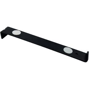
 كتلة تركيب الأرضيات المصفحة مع أربع ميزات للحواف، 15x11.3 سم
KWD 4.500
كتلة تركيب الأرضيات المصفحة مع أربع ميزات للحواف، 15x11.3 سم
KWD 4.500
 ناشر ناشر للضوء من القماش بديل لصندوق الصور، ناشر فلاش للصور قابل للطي، مقاس 50 × 70 سم
KWD 4
ناشر ناشر للضوء من القماش بديل لصندوق الصور، ناشر فلاش للصور قابل للطي، مقاس 50 × 70 سم
KWD 4
 -17%
بطانة داخلية مبطنة لحماية حشوة تخزين الكاميرا
KWD 5
-17%
بطانة داخلية مبطنة لحماية حشوة تخزين الكاميرا
KWD 5