- التسوق ، اصبح سهلا.
- /
- احصل على التطبيق!
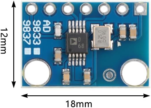
Product parameters
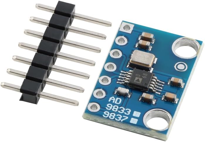
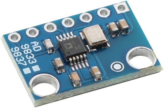
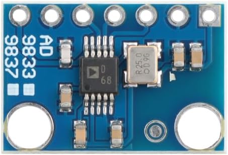
Core chip: ADI original AD9833 DDS frequency synthesizer
Output waveform: sine wave/triangle wave/square wave (programmable switching)
Frequency range: 0.1 Hz-12.5MHz(28MHz clock input)
Frequency resolution: 0.1Hz(28-bit accuracy)
Output voltage: 0-0.6Vpp (sine wave, can be externally amplified)
Clock input: external active crystal (standard 28MHz)
Control interface: SPI communication (up to 40MHz)
Supply voltage: 2.3V-5.5V DC (wide voltage compatible)
Harmonic distortion:-60dBc (sine wave @ 1kHz)
Square wave edge: Working temperature:-40 ℃ ~ 85 ℃
Main functions of the product
Programmable waveform generator based on DDS technology, through the SPI interface precise control of the output frequency (0.1Hz step) and waveform (sine/triangle/square wave). Built-in 28MHz active crystal oscillator, supports 0.1 Hz-12.5MHz signal generation, harmonic distortion as low as-60dBc. Wide voltage power supply (2.3V-5.5V), output impedance 200 , suitable for electronic testing, teaching experiments, sensor excitation and other scenarios.
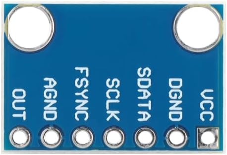
Product main pin function
VCC: The positive pole of the power supply is connected to a 2.3V-5.5V DC power supply (no more than 5.5V is allowed!)
GND: power ground termination system GND
SCLK: SPI clock line to MCU SCK pin
SDATA: SPI data input to MOSI pin of MCU
FSYNC: Chip select terminated GPIO of MCU (active low)
OUT: waveform signal output connected to oscilloscope/amplifier input
SEL: square wave output select disabled when floating, ground enables square wave
REF: reference voltage output can be external precision reference source (default internal 1.21V)

 2PCS 3590S-2-103L 10K أوم دقة السلك الدوار الجرح الدقيق 10K ± 5 ٪ ± 50ppm/℃ 3590
KWD 8.500
2PCS 3590S-2-103L 10K أوم دقة السلك الدوار الجرح الدقيق 10K ± 5 ٪ ± 50ppm/℃ 3590
KWD 8.500
 وحدة USB إلى UART/TTL مع شريحة FT232 وعزل الإشارة لاتصالات البيانات
KWD 6.500
وحدة USB إلى UART/TTL مع شريحة FT232 وعزل الإشارة لاتصالات البيانات
KWD 6.500
 ILI9341 2.8 "SPI TFT شاشة إل سي دي باللمس لوحة 2.8 بوصة شاشة LCD وحدة مجلس 240*320 SPI وحدة عرض مجلس التنمية
KWD 6.500
ILI9341 2.8 "SPI TFT شاشة إل سي دي باللمس لوحة 2.8 بوصة شاشة LCD وحدة مجلس 240*320 SPI وحدة عرض مجلس التنمية
KWD 6.500
 وحدة سلك أقل 433 ميجا هرتز HC-12-SI4438 QFN اتصال تسلسلي طويل المدى نقل بيانات شفاف طاقة منخفضة
KWD 3.500
وحدة سلك أقل 433 ميجا هرتز HC-12-SI4438 QFN اتصال تسلسلي طويل المدى نقل بيانات شفاف طاقة منخفضة
KWD 3.500