- التسوق ، اصبح سهلا.
- /
- احصل على التطبيق!
FEATURES
■High–performance, low–cost CMOS EEPROM–based programmable logic devices (PLDs) built on a MAX architecture (see Ta b l e 1)
■3.3-V in-system programmability (ISP) through the built–in IEEE Std. 1149.1 Joint Test Action Group (JTAG) interface with advanced pin-locking capability–ISP circuitry compliant with IEEE Std. 1532
■Built–in boundary-scan test (BST) circuitry compliant with IEEE Std. 1149.1-1990
■Enhanced ISP features:–Enhanced ISP algorithm for faster programming–ISP_Done bit to ensure complete programming–Pull-up resistor on I/O pins during in–system programming
■High–density PLDs ranging from 600 to 10,000 usable gates
■4.5–ns pin–to–pin logic delays with counter frequencies of up to 227.3 MHz
■MultiVoltTM I/O interface enabling the device core to run at 3.3 V, while I/O pins are compatible with 5.0–V, 3.3–V, and 2.5–V logic levels
■Pin counts ranging from 44 to 256 in a variety of thin quad flat pack (TQFP), plastic quad flat pack (PQFP), plastic J–lead chip carrier (PLCC), and FineLine BGATM packages
■Hot–socketing support
■Programmable interconnect array (PIA) continuous routing structure for fast, predictable performance
■Industrial temperature range
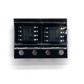 2 قطعة PIC12F683-I/SN SMD 12F683-I/SN SOP-8 PIC12F683-I ميكروكنترولر IC MCU فلاش
KWD 3
2 قطعة PIC12F683-I/SN SMD 12F683-I/SN SOP-8 PIC12F683-I ميكروكنترولر IC MCU فلاش
KWD 3
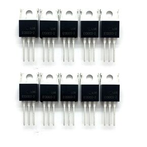 5 قطعة ترانزستور الطاقة MJE13003-2 E13003 E13003-2 ترانزستورات NPN 3A 500V TO-220
KWD 3.500
5 قطعة ترانزستور الطاقة MJE13003-2 E13003 E13003-2 ترانزستورات NPN 3A 500V TO-220
KWD 3.500
 -17%
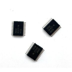
3 قطعة TXS0108 TXS0108EPWR TSSOP-20 8 بت ثنائي الاتجاه مستوى الجهد محول رقاقة المنطق IC
KWD 2.500
-17%
3 قطعة TXS0108 TXS0108EPWR TSSOP-20 8 بت ثنائي الاتجاه مستوى الجهد محول رقاقة المنطق IC
KWD 2.500
 2 قطعة CD4023BE CD4023 TI DIP-14 رقاقة المنطق IC
KWD 3
2 قطعة CD4023BE CD4023 TI DIP-14 رقاقة المنطق IC
KWD 3


