- التسوق ، اصبح سهلا.
- /
- احصل على التطبيق!
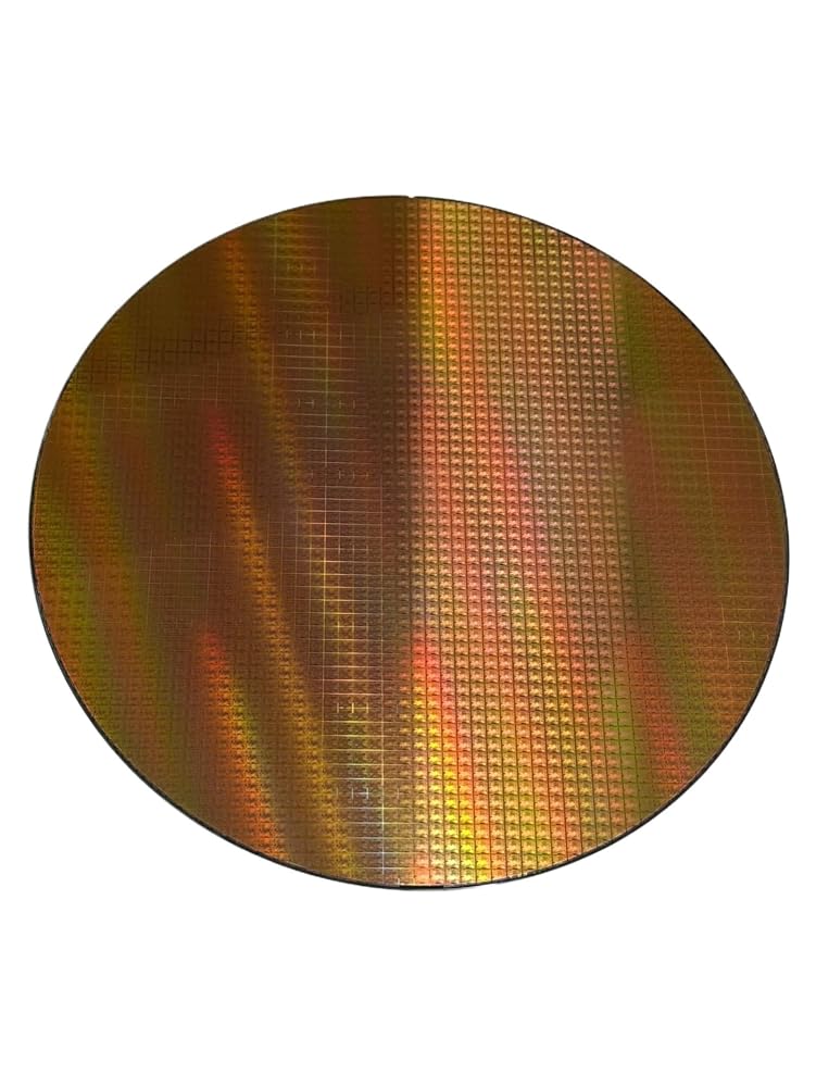
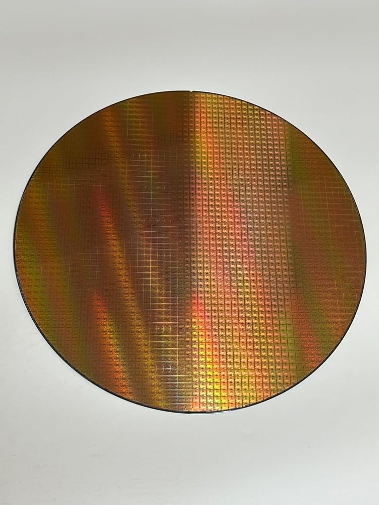
Product DescriptionThis integrated circuit wafer sample features visible semiconductor circuit patterns designed for display, demonstration and educational applications. The patterned surface provides a visual representation of wafer-level circuit layouts used in microelectronics manufacturing.
Suitable for equipment demonstrations, semiconductor training, engineering education and technology exhibitions, the wafer serves as a reference sample for illustrating integrated circuit fabrication concepts and semiconductor processing workflows.
The wafer can be incorporated into laboratory presentations, training programs, exhibition displays and technical showcases where a representative semiconductor circuit sample is needed.
Type: Integrated Circuit Pattern Wafer
Size Options: 8 Inch / 12 Inch
Application: Equipment Demonstration, Semiconductor Training, Technology Exhibition and Educational Display
 GMC04X7R104K16NT -LF - ثابت 2 SMD 04X7R104K16 (100 قطعة قطعة)
KWD 4.500
GMC04X7R104K16NT -LF - ثابت 2 SMD 04X7R104K16 (100 قطعة قطعة)
KWD 4.500
 3.7V متوافق مع البطارية Siemens 42503666817255 ، S30852-D2152-X1 ، V30145-K1310K-X444 ، V30145-K1310-X444 ، V30145-K1310-X445 Gigaset Sl400 ،
KWD 7
3.7V متوافق مع البطارية Siemens 42503666817255 ، S30852-D2152-X1 ، V30145-K1310K-X444 ، V30145-K1310-X444 ، V30145-K1310-X445 Gigaset Sl400 ،
KWD 7
 C5750X7R2A475M - ثابت 2 SMD 5750X7R2A475 (10 قطعة)
KWD 7
C5750X7R2A475M - ثابت 2 SMD 5750X7R2A475 (10 قطعة)
KWD 7
 3.7V متوافق مع البطارية Olympus LI-40B ، LI-42B X-800 ، X-825 ، X-835 ، X-845 ، X-855 ، X-875 ، X-905 ، X-915 ، X-920 ، X-935 ، X-960 ، X-970
KWD 9
3.7V متوافق مع البطارية Olympus LI-40B ، LI-42B X-800 ، X-825 ، X-835 ، X-845 ، X-855 ، X-875 ، X-905 ، X-915 ، X-920 ، X-935 ، X-960 ، X-970
KWD 9